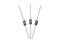
A Schottky diode is a metal semiconductor device made of noble metal (gold, silver, aluminum, platinum, etc.) a as a positive electrode, n-type semiconductor B as a negative electrode, and a potential barrier formed on the contact surface of the two has rectification characteristics. Since there are a large number of electrons in the n-type semiconductor and only a small number of free electrons in the noble metal, the electrons diffuse from the high concentration B to the low concentration a. Obviously, there are no holes in metal a, so there is no diffusion movement of holes from a to B. With the continuous diffusion of electrons from B to a, the electron concentration on the surface of B gradually decreases, and the surface electronegativity is destroyed. Thus, a potential barrier is formed, and the electric field direction is B → a. However, under the action of this electric field, the electrons in a will also generate a drift movement from a to B, thereby weakening the electric field formed by the diffusion movement. When a space charge region with a certain width is established, the electron drift movement caused by the electric field and the electron diffusion movement caused by different concentrations reach a relative balance, and a Schottky barrier is formed.
The internal circuit structure of a typical Schottky rectifier is based on an n-type semiconductor, on which an n-epitaxial layer with arsenic as a dopant is formed. The anode is made of molybdenum or aluminum as a barrier layer. Silicon dioxide (SiO2) is used to eliminate the electric field in the edge region and improve the withstand voltage value of the tube. The n-type substrate has a very small on state resistance and its doping concentration is 100% higher than that of the H-layer. An N + cathode layer is formed under the substrate to reduce the contact resistance of the cathode. By adjusting the structural parameters, a Schottky barrier is formed between the n-type substrate and the anode metal, as shown in Fig. 1. When a forward bias is applied to both ends of the Schottky barrier (the anode metal is connected to the positive electrode of the power supply, and the n-type substrate is connected to the negative electrode of the power supply), the Schottky barrier layer becomes narrow and its internal resistance becomes small; On the contrary, if a reverse bias is applied to both ends of the Schottky barrier, the Schottky barrier layer becomes wider and its internal resistance becomes larger.
To sum up, the structure and principle of Schottky rectifiers are very different from that of PN junction rectifiers. Generally, PN junction rectifiers are called junction rectifiers, while metal half tube rectifiers are called Schottky rectifiers. Aluminum Silicon Schottky diodes manufactured by silicon planar technology have also been developed. This can not only save precious metals, greatly reduce costs, but also improve the consistency of parameters.